
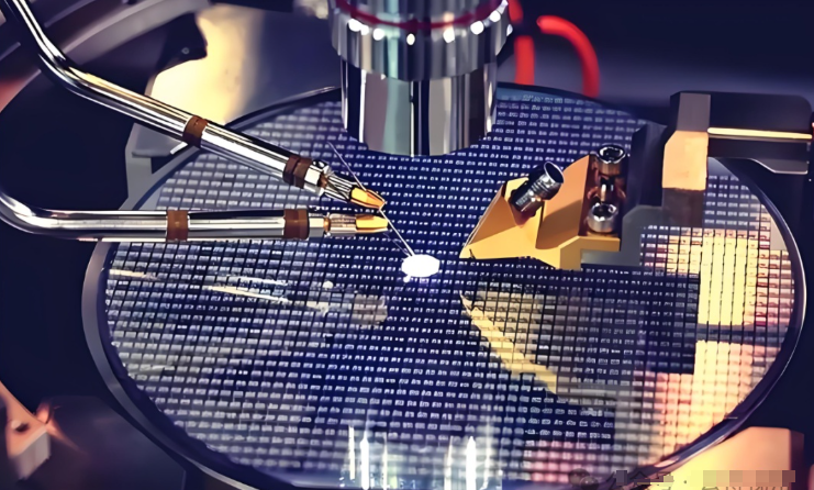
On the fab floor, yield lives and dies on temperature control you can bank on. A drift in the photoresist bake throws off CD uniformity. A hotspot during wafer drying? That’s how you invite micro-defects. And a weak cure in packaging sets you up for delamination. Guesswork doesn’t make the cut. What matters, technically We build thermal systems for semiconductor machinery that hold wafer-level uniformity within ±0.1°C. Halogen, quartz, and short/medium-wave infrared sources deliver fast, clean heating with tight spectral control. The heaters run on Class 1–100 cleanroom power architectures, using low-outgassing materials and zero particle generation across the entire thermal envelope. Repeatability is baked into the control loop: temperature profiles track within 0.5% batch-to-batch, and the thermal budget stays within spec, 24/7. Why this lands in real processes In wafer drying, the system pulls moisture off without surface tension damage, so drying is consistent and scrap drops. In photoresist processing, it hits soft bake and hard bake profiles that stabilize viscosity and adhesion, which tightens lithography overlay and CD control. For packaging, the curing cycle achieves full crosslink without overshoot, so bump integrity and interconnects stay intact. The payoff is predictable throughput, lower energy draw, and fewer maintenance calls. Here is what to keep in mind Matching the lamp spectrum to the coating’s absorption is non-negotiable. We provide application-specific profiles, but tool integration still comes down to chamber geometry and airflow. Commissioning is short—tune lamp power, reflector alignment, and temperature setpoints. Once calibrated, the system holds the line: no unplanned downtime, just repeatable thermal performance.