On the fab floor, a half-degree drift during wafer probing is the kind of thing that turns a good lot into scrap before you even know it happened. When your thermal budget is tight and the schedule doesn’t forgive mistakes, guesswork isn’t an option.
What matters under the hood
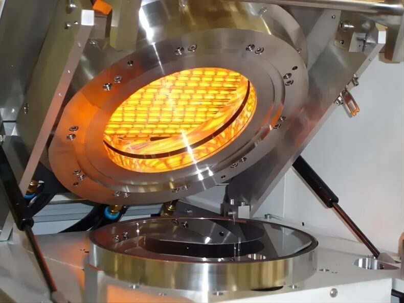
We built the semiconductor wafer probe heater around a short-wave infrared (SWIR) emitter, paired with low-thermal-mass quartz and ceramic assemblies. That gives you sub-second response, and wafer-level uniformity of ±0.1°C across the active area. Run-to-run temperature repeatability is ±0.05°C, so soft bake and hard bake profiles stay locked to the recipe instead of drifting with the shift. The platform is engineered for cleanroom Class 1–100 operation. Surfaces are electropolished and sealed, and zero particle generation is verified by particle counters during qualification. Power delivery holds steady within ±0.2% even when the line voltage moves around, and the heater handles 24/7 duty with zero unplanned downtime in multi-shift lines.
Why this matters in practice
On the probe side, a stable chuck temperature is what keeps parametric data consistent and contact alignment repeatable. In lithography-adjacent bake steps, photoresist chemistry doesn’t forgive overshoot and hot spots—this heater eliminates them, which means fewer defects and less rework. Tighter thermal control also tightens up your setup. Less overshoot means faster stabilization, scrap comes down, and you’re not burning extra energy chasing the setpoint. The payoff is predictable yields and fewer interruptions between lots.
The details that make it work
Installation needs a dedicated, filtered supply matched to the tool’s exhaust and EMI budget. And the probe chuck interface has to be matched to our thermal stack if you want the uniformity we’re quoting. Expect a short commissioning run to calibrate emissivity and map the hot zone to your wafer stack. Once it’s aligned, the process window opens—and stays open.